Anzeige
Anzeige
Anzeige
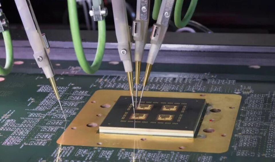
Flying probe in use

In semiconductor manufacturing, precise, reliable tests are crucial - long before the chip moves into the final package. A key component in this: the probe card. It forms the interface between the wafer and the test system. But what happens if this interface itself is faulty?
The answer is simple: nothing good - there is a risk of scrap, production downtime, and manual effort. Those who want to save time and money test their probe cards efficiently - preferably automatically.
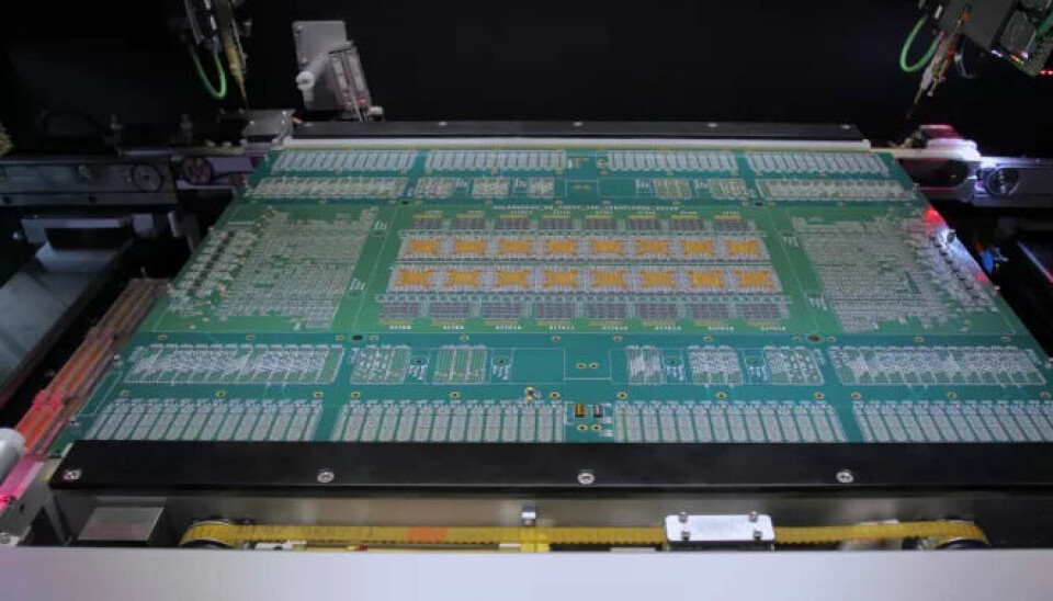
Probe cards (also known as needle cards) connect the tiny contact pads of a wafer with the test equipment. They ensure that electrical signals are precisely transmitted between the test system and each individual die on the wafer. The mechanical challenge: reliably contacting contact pads with only a few micrometers of spacing without damaging them. The electrical challenge: transmitting high-frequency, precise, or power signals without interference.
To fulfill these tasks, modern probe cards are complexly constructed circuit boards with embedded needles, precisely tuned signal paths, RF-optimized materials, and robust mechanical support structures. Depending on the application, the concepts differ - from classic to vertical needle cards to highly integrated MEMS solutions.
The requirements for probe cards are high, making them correspondingly susceptible to errors - already during production, but also later in use. Common sources of error:
Individual failures of this kind are not only difficult to detect - they can also have fatal consequences: for example, when good ICs are sorted out due to faulty tests or defective chips slip through. At this point, it becomes clear: the probe card itself must be tested before it becomes a test tool.
Many manufacturers still use the semiconductor tester itself to test probe cards today. That sounds logical, but it is expensive and inflexible. Why?
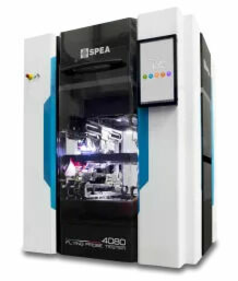
The better way? Separate, specialized test systems, such as those offered by Spea with the flying probe tester.
Spea offers advanced flying probe test systems specifically configured for testing probe cards. These systems enable fully automatic electrical testing without application-specific hardware or manual tests.
Key features of the testers at a glance:
The entire testing process runs on a dedicated platform outside the semiconductor tester - the tester remains available for its actual purpose.
The flying probe systems from Spea are used in all phases of the probe card lifecycle:
The circuit board in the probe card must meet a variety of requirements: high packing density, RF signal quality, thermal stability, and mechanical durability. Spea takes these requirements into account in the measurement technology, for example through:
By integrating these test features, the systems not only detect binary error states but also provide detailed technical condition data.
One of the most important test steps for probe cards is the continuity test across multiple mechanical components, such as connectors, contact blocks, needles, or plug-in PCBs. With the Spea flying probe testers, it is possible to contact different heights simultaneously and precisely.
Testing probe cards with dedicated flying probe systems like those from Spea reduces production risks, improves fault diagnosis, and increases the lifespan of the cards. The systems enable:
For modern semiconductor manufacturers, this means less downtime, lower costs - and a significantly more robust production chain. Spea provides a proven platform for this, which is used worldwide in leading companies.
>> productronica 2025: Hall A1, Booth 255
>> Semicon 2025: Hall B1, Booth 221-1